Nov 05,2015|By
Researchers successfully prepared high quality single crystalline nanostructure (NS) (e.g., particles, nanoribbons or nanowires) of PTCDA on porous anodic alumina oxide (AAO) substrate by the organic molecular beam deposition method, and modulated the morphology, optical and electrical properties of those NS.
Nowadays, organic NS have been widely applied in the optoelectronic device, such as organic light-emitting diodes, organic field-effect transistors, and organic solar cell, as they usually exhibit unique optical and electrical properties superior to those of their bulk counterparts. While the morphology controlled growth, the optical and electrical performance enhancement of high quality organic single crystalline NS still remain a challenge.
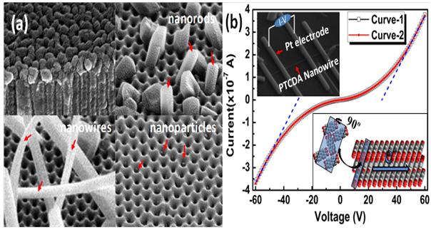
In this study, researchers found that the active sites with smaller curvature radius on AAO promote the nucleation of the NS, and its morphologies can be modulated by controlling the substrate temperatures. The relationships between morphologies and optical properties were investigated in order to deeply understand the optical property modulation mechanism. Electrical conductivity of PTCDA nanowire reaches about 3 0.1 S?m-1, which is much higher than that for polycrystalline films.
This study done by Dr. HAN Yuyan and coworkers in the High Magnetic Field Laboratory, Chinese Academy of Sciences (CHMFL) should have great significance for the better application of organic NS. The results entitled “Preparation, Optical and Electrical Properties of PTCDA Nanostructures” were published in Nanoscale 2015, 7 (40), 17116.
 |
|
(a) SEM images of PTCDA film, nanorods, nanowires and nanoparticles, (b) theI-Vcurves of PTCDA nanowire measured by two-terminal technique, the up and down insets illustrate the measurement schematic and electron flow in PTCDA NW respectively. |
Attachments Download: