Recently the investigators from the High magnetic Field Laboratory, Chinese Academy of Sciences (CHMFL) achieved the manipulation of film microstructure and nano-morphology of high-performance semiconducting polymers, as well as a remarkable enhancement of carrier transport of these materials via magnetic approach.
Effective control of molecular orientation and structural ordering of organic semiconductors (OSs) is crucial to achieve high-performance devices such as organic field-effect transistors (OFETs) and solar cells. The magnitude of magnetic energy of a molecule depends strongly on the direction of the magnetic field relative to the molecular axes, due to the large anisotropy in diamagnetic susceptibility of the molecules (especially pi-conjugated molecules). Therefore the magnetic field can act as a tool to manipulate molecular alignment and packing during the material processing, which becomes potentially a “clean” and universal approach for the control of microstructure and device performance of organic materials.
So far magnetic alignment at high magnetic fields (HMF) has been widely investigated on the molecular or polymer liquid crystals as well as the block copolymers. However structural manipulation via HMF was found to be extremely difficult to date for the highly crystalline molecular semiconductors or semi-crystalline polymers with strong pi-stacking interaction. These OS materials usually possess high carrier mobility and excellent opto-electronic properties.
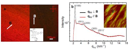
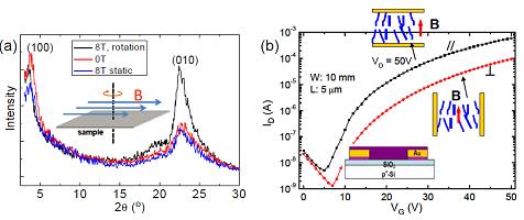
A team led by Prof. ZHANG Fapei in CHMFL, in collaboration with the team of Prof. DAI Jianmin in Institute of Solid State Physics (ISSP) of Chinese Academy of Sciecnces (CAS), achieved via HMF the effective control of film structure of the OSs. For the first time they observed large-area texture structure at centimeter-scale on the films of crystalline (and semi-crystalline) semiconducting polymers by applying a novel solution-cast process at HMF. Microstructural characterizations revealed that the chain backbones of P(NDI2OD-T2), a novel high-mobility polymer utilized in the work, were highly aligned along the applied magnetic field. Based on analysis of the degree of molecular alignment and packing ordering of the films casted from different solvents, the investigators established a mechanism on magnetic alignment, which emphasized that molecular aggregates of P(NDI2OD-T2) pre-formed in the solution initiated magnetic alignment and finally determined the degree of film texture. Furthermore, they utilized the time-modulated magnetic field technique, that is, rotating the sample in the field parallel to the substrate surface in the experiments. Interestingly such processing led to effective control on the orientation of pi-conjugated plane of the backbones, and thus the degree of face-on molecular packing of P(NDI2OD-T2) was enhanced significantly.
The investigators also prepared the OFET device based on the magnetically aligned P(NDI2OD-T2) films. They evidenced a remarkable enhancement of electron mobility by a factor of 4, as well as large mobility anisotropy of 7, compared to the unaligned devices. The good device characteristics (e.g. high on/off ratio) suggested that magnetic alignment processing was compatible to the common OFET fabrication.
P(NDI2OD-T2) is a typical “donor-acceptor” polymer, a class of recently developed organic semiconducting compounds (OSCs) exhibiting the state of art device performance. This study presents a novel and promising route to further improve carrier transport and opto-electronic properties of these materials. It also sheds new light on the understanding of the relationship between the film structure and device performance of OSCs.
The research results entitled “Effective Controlling of Film Texture and Carrier Transport of a High-Performance Polymeric Semiconductor by Magnetic Alignment” were published on Advanced Functional Materials.
The work was supported by “Hundreds Talent Program” of CAS and National Natural Science Foundation of China.
|

|
|
Figure 1 Texture structure of a P(NDI2OD-T2) film cast under HMF (8 Testa): (a) Polarized light micrograph, (b) In-plane graze-incidence X-ray diffraction (GIXRD) patterns. The inset in the left and right figures shows its chemical structure and the AFM topographic image.
|
|

|
|
Figure 2 (a) Specular-scan XRD patterns of the P(NDI2OD-T2) films cast under different HMF conditions. The inset shows geometry of magnetic alignment experiment with the sample rotating in the magnetic field. (b) Typical transfer curves for an OFET device of a magnetically aligned P(NDI2IO-T2) film. |